- Eremex
- Products
- TopoR
- Competitive Advantages
- Improved electromagnetic compatibility
Improved electromagnetic compatibility
TopoR provides the best results for electromagnetic compatibility and interference immunity of PCBs
Smooth, non-bent wires ensure the most “comfortable” path for signals of a PCB
At the place where a conductor makes a 90-degree turn, signal bouncing may occur. This happens mainly due to the change of wire width. At the corner the route width is increased 1.414 times, which results in transfer line parameter discrepancy, and especially to distributed capacitance and self-inductance of the line.
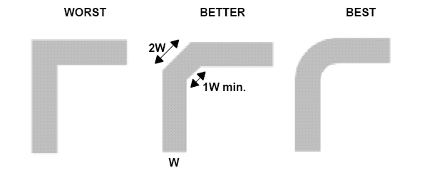 Arc-shaped smoothing prevents signal bouncing resulted by discrepancy of distributed capacitance and self-inductance of the line.
Routing isotropy, minimum wire length and less number of vias provide better electromagnetic compatibility, minimize crosstalks and improve signals quality
If two conductors are positioned close to each other, they cause capacity coupling and reaction coupling between them. Capacity coupling is influencing the conductors which are positioned one above another on the adjacent layers, because they practically create a long anodized-film capacitor.
Absence of preferred routing directions in TopoR CAD system allows to ensure that designed boards have practically no long sections with conductors that are parallel on the adjacent layers. Capability of assigning minimal (in narrow spots) and nominal clearance between conductors significantly reduces the amount and length of narrow spots on the layer. All this coupled with TopoR advantages in overall wires length minimization ensures exceptional characteristics of designed boards in terms of electromagnetic compatibility and interference immunity.
| Other CAD system | TopoR CAD system |
|---|---|
|
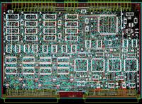
A PCB routed by a high-class Shape-based router: |
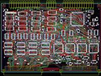
The same board designed by TopoR CAD System: |
|
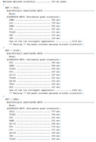
Crosstalk modeling results for this board: |
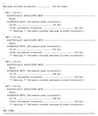
Crosstalk modeling for the PCB routed by TopoR CAD System: |
The modeling results prove that the PCB routed by TopoR provides 10 times better electromagnetic compatibility results.
It is known that each via and the correspondent via-hole add discontinuity to the signal path and involve spray inductance. For example, inductance of a via-hole with 0,4 mm diameter and 1,5 mm height is 1,1 nH. That is why standards for high-speed communication standards tend to have limitations for the allowed number of vias in a signal track.
The unique capabilities of TopoR autorouter for minimizing the number of vias and decreasing the overall wires length allow to improve the quality of electric signals on a printed circuit board.
The algorithms used by TopoR CAD System allow to reduce the influence of PCB material on electrical parameters of signal tracks
In case the designed board contains contemporary high-speed interfaces, it is necessary to consider influence of the PCB material to electrical characteristics of conductors. As is known, a PCB includes a base consisting of a braided fiberglass structure secured by epoxide filling compound.
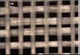
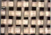
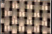
Typical structure of fiberglass PCB base material
If conductors of a differential pair are parallel to braiding of fiberglass so that one of them passes mostly above the fiberglass, while the other passes mostly above the epoxide material, then the characteristics of these conductors become different. This happens because of inequality of dielectric capacity of fiberglass (approximately 6) and epoxide material (3). This results in deference between the signaling speed in different conductors of a differential pair. Thus the receiving side experiences worse capabilities for transmitted signal identification as well as a general interference.
 Timing desynchronization for differential signals is caused by the different dielectric constant of two wires of differential pair. This can complicate the recognition of transmitted logic state on the receiving side.
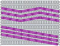
There exist several rather complicated and expensive ways of solving this problem. They include routing of high-speed differential pairs with dog-legs to avoid strictly vertical or strictly horizontal sections.
Intel’s recommendations for routing high-speed differential pairs.
Generally this requires diligent manual routing and does not allow to completely solve the problem in case of using BGA routing of cases made by templates. This results in forming horizontal and vertical areas with up to 5 cm length.
TopoR autorouter does not have preferred routing directions both in the area of BGA components and in the other areas of a PCB, thus being able to solve this problem “automatically”.

